Design for test (DFT) is a methodology for silicon integrated-circuit chips to enable devices to be tested during and after manufacture. Such testability permits the detection of faults due to problems in the manufacturing processes that would adversely affect the functional behaviour of the device. This note explains the concepts of a particular DFT methodology called scan test, which modifies the logic of a design in such a way that the functional behaviour is preserved but classes of faults become detectable.
Scan chains
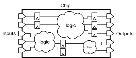
A chip can be viewed as a set of input ports that feed into a series of combinatorial and sequential cells, and arrive at a set of output ports. To test that the function of the chip is correct, it would suffice to check that a particular output is generated for a particular input, or sequence of inputs and outputs. However, if the intervening logic contains sequential elements, is computationally difficult to setup inputs each clock cycle to observe desired values on all outputs. Doing so requires sequencing of state transitions through the logic, but the size of the state space grows exponentially with the number of states.
To avoid an intractable state space, the design is changed so that inputs and
observable outputs are separated only by combinatorial logic. This is done by
adding new controllable primary inputs and observable outputs, called
scan chains. A scan chain adds three ports to the chip: a scan chain input,
scan_in, a scan chain output scan_out and an enable scan_enable.
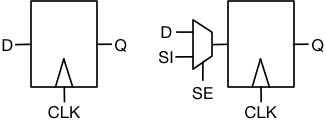
All registers are converted by adding a multiplexer on the D pin, with one
input connected to the data signal. The first scan-chain register has it’s
other multiplexer input connected to scan_in. Subsequent scan registers
take their other multiplexer inputs from the output of the previous register in
the chain. The final register in the chain drives scan_out from it’s D pin.
All multiplexers are controlled by scan_enable.

When scan_enable is pulled high, and the clock pulsed, data is shifted into
each register in the chain. Each bit of a chain of N registers can be set in N
clock cycles. When pulled low, the chip is in normal functional mode. These
inputs allow a simple test procedure to be implemented:
- Set
scan_enablehigh (scan mode). - Shift in N bits of input data.
- Set
scan_enablelow (functional mode). - Tick the clock once to propagate input vector though combinatorial logic into outputs.
- Set
scan_enablehigh (scan mode). - Shift out N bits of output data.
- Check that the output data equals the input data transformed by the same logic function.
Since typical tests will contain large numbers of patterns, the time to test
one pattern is critical. It is determined by the length of the chain, to shift
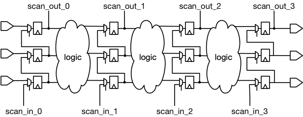
in and out data. To reduce test time, additional scan chains can be introduced
to allow shifting to be performed in parallel. Each chain adds scan_in and
scan_out ports to the chip. The number of scan chains is chosen to trade
off the physical requirements of the additional ports and routing with test
time and coverage. To avoid many additional ports at the top level, a set of
parallel scan chains can be driven by DFT logic that supplies compressed
patterns to the inputs and compresses results from the outputs.
Wrapper chains
Typically, a chip is too complex to test with a single set of scan chains. Even with only combinatorial logic between primary inputs and observable outputs, it becomes computationally difficult to analyse to generate patterns that can effectively exercise it to achieve good coverage and fault isolation. Instead, a chip is divided into sub components, each of which is amenable to testing (an approach known as hierarchical DFT). The components are referred to as test cores and typically naturally correspond to functional blocks of the chip design.
It is necessary for a test core to be isolated from the rest of the design. At a chip-level primary inputs are controllable in that their values are always known. However, the values of an input to a test core are unknown and likely to be Xs. If X values propagate into a test core, coverage can be reduced, or worse, the testing methodology may be invalidated altogether. Isolation is achieved with wrapper chains that are inserted between the IO ports and the core logic of the design. A bypass multiplexer is inserted on the output of the wrapper scan register to control whether the input or output is used or driven respectively. If the input or output is directly connected to a register, then a bypass is not necessary.
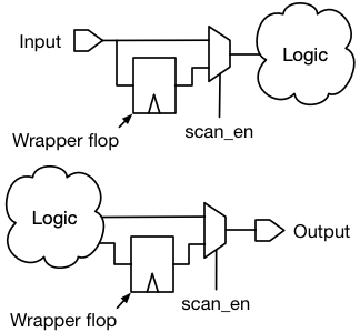
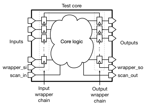
An input wrapper chain is the chain of registers that capture the primary
inputs to the core, with their D inputs corresponding to each input of the test
core. Some inputs may be omitted from the wrapper chain, such as clock, reset
and test-related signals. Input wrapper chains are different to regular scan
chains only in the way that their scan_enable is controlled. During test mode,
the scan enable of the input wrapper is held high when the regular scan_enable
is low and all other registers are in functional mode. The effect of this is
that the input wrapper chain continues to shift in known values, rather than Xs
from outside of the test core. When the input wrapper registers are not shared
with any other test core, the captured values can be shifted out with the other
test pattern results to ensure all of the registers are functioning correctly.
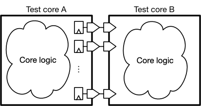
An output wrapper chain behaves exactly as an internal scan chain during test
mode. However, when they are shared with an adjacent test core, their
scan_enable is controlled differently since they will function as an input
wrapper chain for that core, with the behaviour described above.
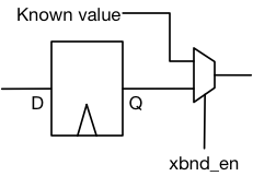
X bounding
It may not be possible to add all registers into the scan chains for a design.
In this case, to prevent Xs from propagating into the logic during test, all
sources of Xs must be masked with known values. This is done by inserting a
multiplexer to take the Q pin as input, with the other input as an alternative
known value, typically from a register on a scan chain. The multiplexer is
controlled by an xbnd_enable signal, which when set high will prevent X
propagation during test mode, and otherwise maintains the functional behaviour
of the circuit.
References / further reading
- Design for testing (Wikipedia)
- DFT, Scan and ATPG (VLSI Tutorials)
- Automatic test pattern generation (Wikipedia)
- Stanford EE371, lecture 14: Design for testability
Acknowledgements
Thanks to Evan Griffiths for his detailed explanations of DFT insertion, upon which this note is based.